特点:
Live MOS感光器件在画面素质可以媲美全祯(FFT) CCD,低功耗上则可媲美CMOS。
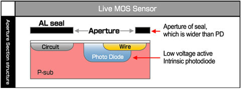
简化的电路使得光电二极管到微透镜的距离缩短,从而保证了优秀的敏感性和大入射角的画面质量。
1、分辨率:7.5MP,具有优秀的低照度性能特性;
2、增益:采用了低躁声技术,降低颗粒性;
3、影调范围:简化了寄存器和其他电路,使得FFT-CCD感光二极管的感光面积更大,提高了灵敏度和提高响应速度;
4、低功耗:其功耗大约是FFT-CCD的一半;
5、高速:简单的电路结构提高了整体的处理速度。
重新设计的感光器件具有更大的感光表面
感光区域大约是感光元件表面的30% (与CCDs相比)。Live MOS感光器件的优点是:简单电路要求和更薄的NMOS结构层,从而提供了更大的感光区域。而且,电路技术的改进提高了感光效率和改进了图象素质。
新型的光电二极管读出传输机理,将电路通道的数量减少到两条(同CCD感光器件),从而使得不参与感光的区域变小。通过有效地扩大感光区域,使得捕捉光线的能力加强,在保证了高灵敏度的同时也保证了画面素质。同时,已经研制了新的低躁声光电信号放大电路,将用于以后的灵敏度改进。
低躁声技术大幅度地改进了低照度下的影象素质
在5V(设计电压:2.9V)低压系统中,采用的专用处理技术,大大地降低了躁声。考虑了工作信号躁声,感光光电二极管深嵌入硅片中,与芯片表面上产生噪声的元件相隔离。使得图象更为清晰,抑制了在低照度下拍摄经常出现得颗粒性和写噪声。这项技术整体改善了低照度下的性能,在低照度下拍摄的画面更为清晰。
英文版
Live MOS Sensor
Features
The Live MOS Sensor offers image quality comparable to a Full Frame Transfer (FFT) CCD sensor with the low power requirements of a CMOS sensor, and is noteworthy for its high-quality imaging capabilities over an extended period of time. Simplified circuitry that reduces the distance from each photodiode to its corresponding on-chip microlens assures excellent sensitivity and image quality even when light strikes it at a high angle of incidence.
-
Resolution: 7.5 megapixels, with excellent low-light performance characteristics.
-
Grain: low-noise technologies assure reduced graininess.
-
Tonal range: Simplification of the transfer register and other circuitry results in a large photodiode surface area for FFT-CCD-level sensitivity and responsiveness.
-
Low power consumption: Power requirements are approximately half those of FFT-CCD sensors.
-
High speed: Simple circuit structure contributes to faster processing overall.
Redesigned Sensor Elements with Greater Photosensitive Surface Area
Photosensitive area accounts for 30% of sensor element surface (comparable to CCDs). The Live MOS Sensor takes advantage of the simplified circuit requirements and thinner layer structure of NMOS type sensors to offer a larger photosensitive surface area. In addition, circuit technology refinements were made to boost light utilisation efficiency and improve image quality.
A new transfer mechanism for photodiode signal readout enabled us to reduce the number of circuit paths to two, the same as in a CCD sensor, and thereby minimise the surface area that is unresponsive to light. By effectively enlarging the photosensitive surface area and enabling it to capture light that was previously lost, we were able to achieve both high sensitivity and superior image quality. We also developed a new low-noise photodiode signal amplification circuit to further improve sensitivity.
Low-Noise Technology for Significantly Improved Imaging in Low-Light Environments
A dedicated processing technology developed for use in 5V (design specifications: 2.9V) low-voltage systems is employed to significantly reduce noise. Operating signal noise was also considered, and the sensor photodiodes were deeply embedded in silicon to isolate them from noise-causing elements on the chip surface. As a result, images are clearer, and the graininess and white noise that often appear when shooting in low light are suppressed. Thanks to this technology, low-light performance is improved overall, and a clear image can be obtained even when shooting in very dim light.
|